
Why Semiconductor Laboratories Must Implement Antistatic Flooring
2025-03-24
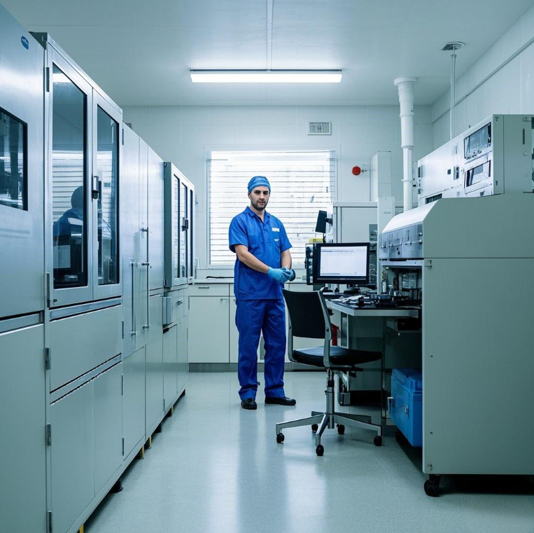
In semiconductor manufacturing and research, precision and reliability are paramount. Even minor disruptions can lead to costly defects, compromised product quality, and safety hazards. Among the critical threats facing these environments, electrostatic discharge (ESD) ranks as one of the most insidious. This article explores why antistatic flooring is a non-negotiable component of semiconductor laboratories, detailing its role in protecting sensitive electronics, enhancing operational efficiency, and ensuring compliance with global standards.
1. The Devastating Impact of ESD in Semiconductor Laboratories
The Scale of the Problem
Semiconductor devices, such as integrated circuits (ICs), microchips, and printed circuit boards (PCBs), are highly vulnerable to ESD. A single discharge as low as 100 volts can irreparably damage these components, even if imperceptible to humans. According to the Electrostatic Discharge Association (ESDA), ESD accounts for up to 30% of semiconductor failures, costing the industry billions of dollars annually in rework, scrap, and delayed production.
Semiconductor devices, such as integrated circuits (ICs), microchips, and printed circuit boards (PCBs), are highly vulnerable to ESD. A single discharge as low as 100 volts can irreparably damage these components, even if imperceptible to humans. According to the Electrostatic Discharge Association (ESDA), ESD accounts for up to 30% of semiconductor failures, costing the industry billions of dollars annually in rework, scrap, and delayed production.
How ESD Occurs
Static charges accumulate through friction (e.g., walking on non-conductive flooring, handling materials) or induction (e.g., proximity to charged objects). When discharged, these charges can:
Static charges accumulate through friction (e.g., walking on non-conductive flooring, handling materials) or induction (e.g., proximity to charged objects). When discharged, these charges can:
- Burn microscopical pathways in silicon wafers.
- Degrade oxide layers, reducing device lifespan.
- Induce soft errors in memory chips, corrupting data.
- Trigger thermal runaway, causing catastrophic failure.
The Hidden Cost of ESD
Beyond immediate damage, ESD can create latent defects that manifest later in the supply chain, leading to warranty claims, brand reputation losses, and regulatory fines. For example, a faulty IC in a medical device could endanger patient safety, while a flawed chip in an automotive system might cause recalls.
Beyond immediate damage, ESD can create latent defects that manifest later in the supply chain, leading to warranty claims, brand reputation losses, and regulatory fines. For example, a faulty IC in a medical device could endanger patient safety, while a flawed chip in an automotive system might cause recalls.
2. The Role of Antistatic Flooring in ESD Mitigation
Key Functions of Antistatic Flooring
Antistatic flooring acts as the first line of defense against ESD by:
Antistatic flooring acts as the first line of defense against ESD by:
- Dissipating Static Charges: Maintaining a surface resistivity of 10⁶–10⁹ ohms, it channels charges to ground safely.
- Controlling Charge Generation: Reducing friction between footwear and flooring to minimize static buildup.
- Creating a Grounded Environment: Integrating with grounding systems (e.g., copper grids) to ensure continuous conductive paths.

Material Selection for Semiconductor Labs
Semiconductor environments demand flooring that balances conductivity, durability, and cleanliness:
Semiconductor environments demand flooring that balances conductivity, durability, and cleanliness:
- Conductive Rubber: Shock-absorbent and chemical-resistant, ideal for heavy equipment.
- Low-Outgassing Vinyl: Minimizes particle emission in cleanrooms.
- Ceramic Tiles: Heat-resistant and non-combustible for high-temperature processes.
- Metal Composite Flooring: Provides superior conductivity for extreme ESD protection.
Compliance with Standards
Leading organizations like the International Electrotechnical Commission (IEC) and ESDA mandate antistatic flooring in semiconductor facilities. Compliance with standards such as IEC 61340-5-1 and ANSI/ESD S20.20 ensures:
Leading organizations like the International Electrotechnical Commission (IEC) and ESDA mandate antistatic flooring in semiconductor facilities. Compliance with standards such as IEC 61340-5-1 and ANSI/ESD S20.20 ensures:
- Uniform resistivity across the lab.
- Proper grounding to prevent charge accumulation.
- Worker safety through controlled discharge rates.
3. Unique Requirements of Semiconductor Laboratories
Cleanroom Compatibility
Semiconductor labs often operate in ISO Class 4–8 cleanrooms, where particle contamination is strictly regulated. Antistatic flooring must:
Semiconductor labs often operate in ISO Class 4–8 cleanrooms, where particle contamination is strictly regulated. Antistatic flooring must:
- Be seamless or tightly bonded to prevent particle infiltration.
- Resist chemicals used in wafer processing (e.g., acids, solvents).
- Support airflow systems without disrupting laminar flow.
Temperature and Humidity Control
ESD risks increase in low-humidity environments (<30% RH). Antistatic flooring must remain effective across temperature ranges (18–24°C) and humidity fluctuations, often requiring integrated humidity sensors and HVAC system integration.
ESD risks increase in low-humidity environments (<30% RH). Antistatic flooring must remain effective across temperature ranges (18–24°C) and humidity fluctuations, often requiring integrated humidity sensors and HVAC system integration.
Compatibility with Equipment
Heavy machinery, robotic arms, and wafer-handling tools generate vibrations and mechanical stress. Flooring materials must:
Heavy machinery, robotic arms, and wafer-handling tools generate vibrations and mechanical stress. Flooring materials must:
- Absorb shocks to protect delicate equipment.
- Resist indentation and wear from rolling carts and automated guided vehicles (AGVs).
4. Case Study: Antistatic Flooring in a Leading Semiconductor Fab
Challenge
A major semiconductor manufacturer experienced a 22% defect rate in its IC production line due to ESD. Traditional flooring and wrist straps were insufficient to address charge accumulation from personnel movement.
A major semiconductor manufacturer experienced a 22% defect rate in its IC production line due to ESD. Traditional flooring and wrist straps were insufficient to address charge accumulation from personnel movement.
Solution
Implementing conductive rubber flooring with embedded copper grids, bonded to a central grounding system. The flooring:
Implementing conductive rubber flooring with embedded copper grids, bonded to a central grounding system. The flooring:
- Achieved a surface resistivity of 8 × 10⁶ ohms.
- Integrated with an IoT-enabled monitoring system to track real-time charge levels.
Results
- Defect rates dropped to 3% within six months.
- Annual savings of $4.2 million from reduced rework and scrap.
- Compliance with SEMI S2-0203 (safety guidelines for semiconductor manufacturing).
5. Installation and Maintenance Best Practices
Pre-Installation Steps
- Subfloor Preparation: Ensure smoothness, dryness, and flatness to prevent bonding failures.
- Environmental Testing: Verify humidity (40–60%) and temperature stability.
Installation Process
- Apply a conductive primer to enhance adhesion.
- Lay flooring tiles with conductive adhesive, ensuring 100% coverage.
- Connect tiles to a grounding grid using copper tape or wires.
- Test resistivity at 1-meter intervals to confirm uniformity.
Maintenance Strategies
- Daily Cleaning: Use microfiber mops and ESD-safe detergents.
- Monthly Inspections: Check for cracks, delamination, and grounding integrity.
- Annual Resistivity Testing: Ensure compliance with industry standards.
6. Beyond Flooring: Holistic ESD Protection
While antistatic flooring is critical, it must be part of a comprehensive ESD control program:
- Personnel Training: Educate staff on ESD risks and proper protocols.
- Conductive Workbenches: Use grounded work surfaces for assembly.
- ESD-Protective Packaging: Shield components during transportation.
- Humidity Regulation: Maintain optimal humidity to suppress static buildup.
Conclusion
In semiconductor laboratories, where the margin for error is measured in nanometers, antistatic flooring is not a luxury—it is a necessity. By investing in high-quality, properly installed flooring systems, organizations can protect their assets, reduce operational costs, and uphold safety and compliance standards. As the industry continues to advance toward smaller, more sensitive devices, the importance of robust ESD protection will only grow, solidifying antistatic flooring as a cornerstone of semiconductor innovation.
How To Install Homogeneous Vinyl PVC Flooring
Applications and Installation Essentials of Antistatic Flooring
Related Article

PVC flooring has become a popular flooring choice for homes, hospitals, schools, offices, and other commercial spaces due to its durability, water resistance, and easy maintenance. However, proper cleaning is essential to maintain its appearance and extend its service life.
How to Clean PVC Flooring: A Complete Guide to Daily Cleaning and Maintenance
Homogeneous flooring, homogeneous vinyl flooring, through-body homogeneous flooring, anti-bacterial homogeneous flooring, chemical resistant homogeneous flooring, medical grade flooring, seamless hygienic flooring, high traffic institutional flooring
Through-Body Homogeneous Flooring – Anti-Bacterial Chemical Resistant Homogeneous Vinyl Flooring for Medical, Laboratory and High-Traffic Institutional Spaces
Homogeneous flooring, homogeneous vinyl flooring, through-body homogeneous flooring, anti-bacterial homogeneous flooring, chemical resistant flooring, medical grade homogeneous flooring, high traffic institutional flooring, seamless hygienic flooring
Through-Body Homogeneous Flooring – Anti-Bacterial Chemical Resistant Homogeneous Vinyl Flooring for Medical, Laboratory and High-Traffic Institutional Spaces
Homogeneous flooring, homogeneous vinyl flooring, through-body homogeneous flooring, anti-bacterial homogeneous flooring, stain resistant homogeneous flooring, hospital flooring, laboratory flooring, high traffic public flooring
Full Through-Body Homogeneous Flooring – Anti-Bacterial Stain Resistant Homogeneous Vinyl Flooring for Hospital, Laboratory and High-Traffic Public Areas